Apple A9X SoC: Chipworks teardown reveals some interesting specs
With the release of the iPad Pro, Apple officially introduced its A9X chip, powering a device twice as fast as its A9 counterpart powering the iPad Air, while leaving the A8 chip powering the iPhone 6S in a trail of dust. This is according to the latest Thanksgiving teardown from Chipworks.
Some of the information that surfaced from the teardown revealed a few surprises that weren’t apparent in the wake of the launch of the iPad Pro, particularly in reference to specs and performance. Initially, the information was limited due to the fact that preliminary assessments were made using software benchmarks only, without an internal look at the chip itself.
First of all, the ARM chip, manufactured by TSMC, uses a 16nm FinFET process, bringing the chip to roughly a 147(square)mm die size. With that said, the A9X is officially the largest chip in the A-series, followed by the A5 phone SoC.
GPU performance explained
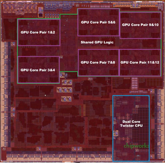
It’s no secret that the iPad Pro’s graphic performance has proven to be on a whole different level compared to any previous iPad. This is the result of the A9X chip’s 12 GPU cores cluster, otherwise defined as PowerVR Series7XT, manufactured by Imagination. The 12 core design for the iPad Pro’s GPU offers a few clues about what Apple intends to do with future iterations of the A-chip. In reference to die-size, the additional space provided for the GPU cores can only means future plans of providing more power to graphic applications, possibly in the realm of both gaming and productivity.
This is especially relevant in light of the fact that both Adobe and Microsoft have designed their creative and productivity apps by taking into serious consideration the larger real estate provided by the iPad Pro’s display, as well as stylus input.
According to Chipworks, it’s also entirely possible that Apple may have been working on its own design for the PowerVR GPU since at least the A4 chip and its SGX 533.
Memory controller
The A9X chip also integrates a 128-bit LPDDR4 memory controller, which is designed to provide twice as much memory bandwidth to support the 12 core GPU cluster, for a whopping total of 51.2 GB per second. While it may seem overkill, special consideration must be given to the 12 cores powering graphically intensive applications like Adobe apps and Microsoft Office 2016, as well as other production apps for image manipulation and multimedia.
Speaking of memory, another interesting find was that the A9X chip does not include L3 cache at all, leaving only the L1 and L2 cache tu support the CPU and GPU, as well as a number of low level cache amounts for a number of other functional blocks.
According an assessment of Chipworks findings from Anandtech, an explanation for getting rid of the L3 cache can justified by power requirements. As Anandtech’s Andrei Frumusanu explains in his own determination of the chip, there is no obvious reason for Apple to not include L3 cache in the A9X chip, as the difference would be minimal.